


产品中心
为中国企业客户提供专业优质的服务
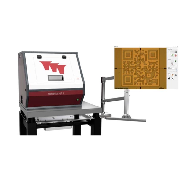
Microwriter ML3 Pro
MicroWriter ML3 Pro is our flagship machine and is a compact, highperformance, direct.write optical lithography machine which is designed to offer unprecedented value formoney in a small laboratory footprint. lt also has an excellent environmental footprint:power consumption of the machine even when exposing is comparable to that of a laptop.
产品描述
Sitting on its own vibration-isolation optical table, its only service requirement is astandard power socket. A temperaturecompensated light-excluding enclosure with safetyinterlock allows it to be used equally well in an open laboratory environment or in a cleanroom. Easy to use Windows® based software means most exposures can be set up andlaunched with just a few mouse clicks. Four different minimum feature sizes (0.6um, lum.2um and 5um) can be selected automatically via software. This allows non-critical parts ofthe exposure to be performed rapidly while retaining high resolution writing for criticalparts. An additional 0.4um minimum feature size is available as an option. The MicroWriterML@3 Pro features an optical surface profilometer tool and an automated wafer inspectiontool for examining fabricated structures. A backside alignment camera with real-timeimages for aligning double-polished wafers is available as an option.
产品参数
MicroWriter ML3 Pro system
a. 195mm x 195mmmaximumwriting area.
b. 230mm x 230mmx15mmmaximumwafersize.
c. 0.4um, 0.6um, 1µm, 2um and 5um minimum feature size across full writing area.
d. 385nm Dual wavelength lightsource- software selectable 1.1 Microwriter ML3 Pro system
e. Extremely fast writing speed- up to: 15mm2 /minute (0.6µm minimum feature size), 50mm2 /minute (1µm minimum feature size), 120mm2 /minute (2µm minimum feature size) and 180mm2 /minute (5µm minimum feature size). These allow a typical 50mm x 50mmarea combining critical and non-critical areas to be exposed in under 30 minutes or a typical 100mm x 100mm area to be exposed at 2µm minimum feature size in under 2 hours.
f. Optical autofocus system using yellow light with real-time surface tracking module–no minimum wafer size.
g. High quality infinite conjugate optical microscope with x3 aspheric objective lens, x5 and x10 Olympus plan achromatic objective lens, x20 Olympus plan apochromat objective lens, and yellow light illumination for alignment to lithographic markers on the wafer (±0.5µm 3σ alignment accuracy). x50 Olympus plan apochromatic objective lens.
h. Grey scale exposure mode for 3-dimensional patterning (up to 768 grey levels).
i. Built-in 2-dimensional optical surface profiler (100nm thickness resolution) for examining exposed resists and MEMS process steps.
j. Virtual mask aligner (VMA): Allows pattern to be exposed to be displayed in real-time on top of the microscope image, allowing the user to see precisely where pattern will be exposed.
k. Bulls-eye tool can automatically identify the precise position of lithographic markers visible under the real-time microscope.
l. Temperature compensation module, keep the substrate temperature fluctuation inside the device within 0.25℃.
m. Optical table (with integration of PC, monitor and keyboard).
n. Clewin mask design software, Acceptable file formats: CIF, GDS2, BMP, TIFF, JPEG, PNG, GIF; Oasis, DXF, Gerber RS-274X acceptable via KLayout conversion.